")
")
")
Correlation of physical and physicochemical properties of semiconductor, dielectric and ferroelectric materials with optical, electrical, electrochemical and other functional properties.
Application of various processing methods that allow to modify the crystal structure of particles, especially the ratio of surface and structural defects, towards improving the functional properties of semiconductor, dielectric and ferroelectric materials used as photo(electro)catalysts, selective electrochemical sensors for the identification of pollutants and moisture, biosensors, inert coatings, etc.
Research focuses:
- Oxide semiconductor materials.
- Dielectric and ferroelectric materials based on perovskites
- Materials based on calcium phosphate.
- Crystal structure with emphasis on defects in the crystal lattice.
- Infrared, Raman, photoluminescence and UV-Vis diffuse reflectance spectroscopy, impedance spectroscopy.
- Methods for thermal characterization TG/DTA, DSC, dilatometry
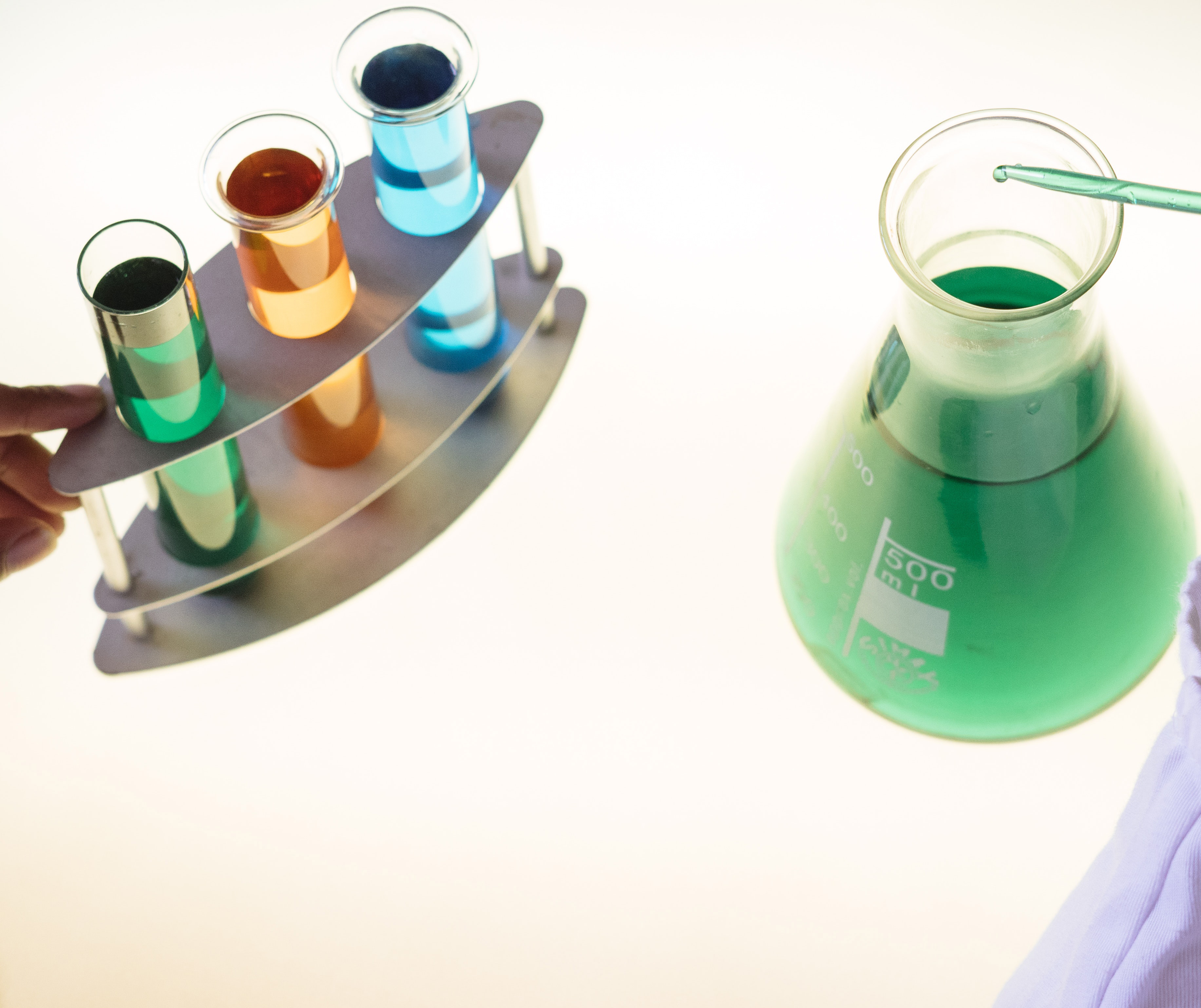
- Photo(electro)catalysts, selective electrochemical sensors, biosensors.
- Mathematical and computer modeling, thermodynamics and kinetics of high-temperature processes in materials based on silicon and aluminum
 Group for nanostructured optically active materials and semiconductors
 Group for biomedical engineering and nanobiotechnology
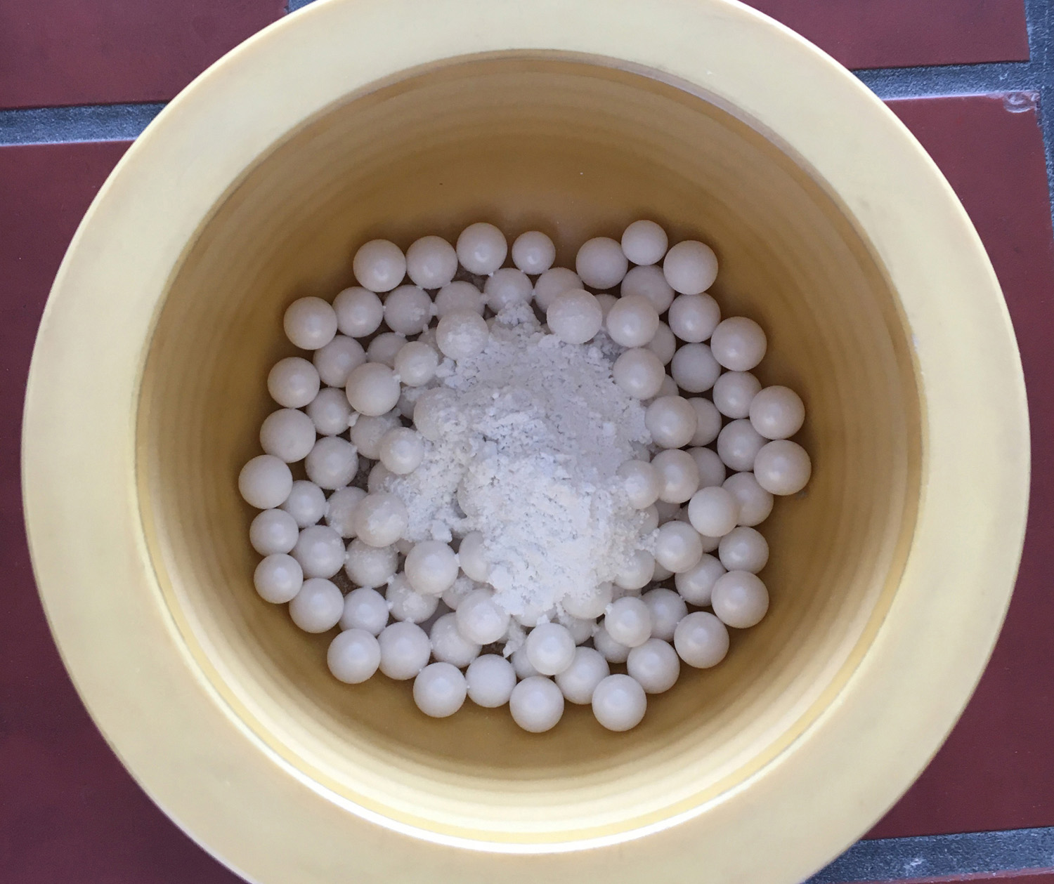 Group for multifunctional ceramics, sintering and composite materials
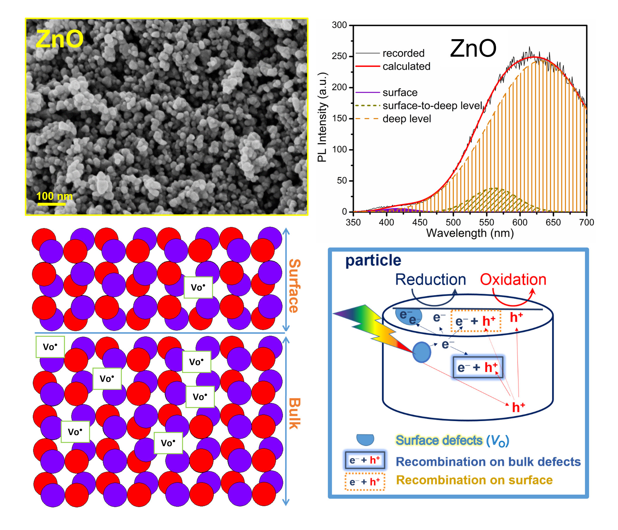 Group for the correlation of properties and functional characteristics of condensed matter